2.4.2000 News from the LGP-30
("No. 4 lives")
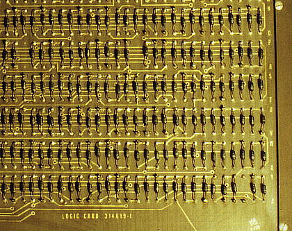
The logic board and netlist
A brief note at first: In the meantime we had tested all diodes on the original logic board twice and found the defective diode that was the cause for the faulty behaviour of the Y and R instructions.
For the rest, we created practically a complete netlist of all connections between the individual modules and the schematics of all modules (with the exception of the two modules in the scope display unit). We also know all 140 connections of the logic board, and the diodes that are connected to the outside, and approximately the half of the connections between the diodes.
Topic schematic: A complete schematic of the computer would be an impressive diligent piece of work you could decorate your wall with, but it would be totally unhelpful because of its size and complexity. We therefore concentrated on netlists that are more abstract and have the advantage of being searchable with a text editor as they are ASCII files. Where it would be helpful a partial schematic can always be created, though.
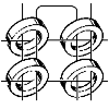
Portion of the logic board
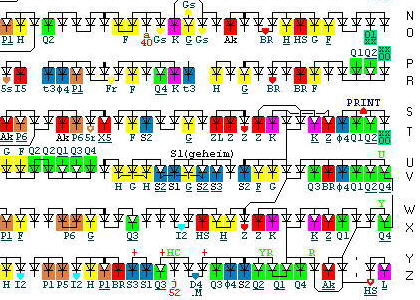
The same portion
(diodes N33 .. Y60) in a more abstract form
In the colourfil picture the expert immediatly recognises the following: The diodes Y48 to Y52 (all diodes are always labelled with the coordinates of their anodes) form an AND gate and decode the instructions Y (address replacement) and R (return address) during phase 4, the execution phase.
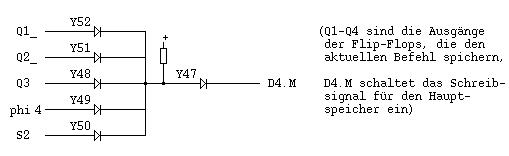
Q1 to Q4 are the outputs of the flip-flops that hold the instruction.
D4.M enables the write signal for the memory
The differenciation between the two instructions is done via W60, W59, Y56 and Y57 that - if Q4 = 1 - apply the contents of the accumulator to the input of the memory write amplifier, or via Y53 and Y54 that - if Q4 = 1 - apply the output of the address incrementer to the input of the write amplifier. However, the write amplifier is only active during phase 4 and due to S2 only during the time when the address part of an instruction is present.