General
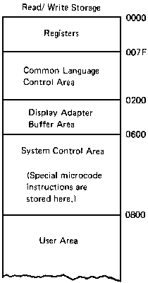
The main memory or RAM is called Read/Write Storage (short:
RWS) by IBM. The RWS is located on module cards M2, M4, N2 and N4, depending
on the installed options, in this order. Each card has a capacity of 16kB.
Memory data flow
When reading data from RWS the information is gated over the Storage R/W
bus to the processor and, if Cycle Steal is active, to the display
adapter.
Data to be written into RWS is gated over the same bus from the processor to
RWS.
Memory addressing
Memory (RWS or ROS) is addressed with the help of the Storage Address
Register (SAR). The meaning of the individual address bits is shown
in the following picture:
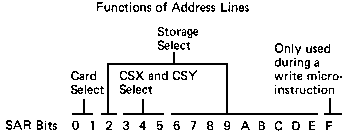
Be careful that the bits are counted from left to right so that bit 0 is
the most significant bit and bit 15 is the least significant bit!
If bits 0 to 8 are all zero the processor registers are addressed instead
of RWS.
Bits 0 and 1 select one out of four memory cards, (0 0) selects card 0 or M2,
(0 1) select card 1 or M4 and so on. Bits 3 to 5 are taken as chip select
signals for the memory chips. The remaining bits address one specific bit
of the selected chip.
A detailed wiring can be found in the
memory diagram
.