The following description of the processor is based on the
data flow chart.
General
- Data Bus In/Data Bus Out
The data bus transfers a byte plus one parity bit (nine bits in total) from and
to the Base I/O-Karte.
- Storage Address Bus
The 16 bit address bus.
- Storage R/W Bus
This is the 18 bit data bus which transfers two bytes of data with one parity
bit for each byte.
Internals
- Read Data Register (RDR)
This 18 bit data register latches all words coming from the data bus.
- Storage Address Register (SAR)
This 16 bit register is used for addressing the storage.
- Operation Register (Op Reg)
The instruction register (16 bits) contains the instruction to be decoded.
- Storage Data Register (SDR)
This 8 bit register takes data from the external data bus (Data Bus In) and
also serves as second operand for the ALU.
- Arithmetic Logic Unit Register (ALU Reg)
This is the first operand for the ALU and also the output data register for
the external data bus (Data Bus Out).
- Arithmetic Logic Unit (ALU)
There's where calculations are done! The ALU is 8 bits; it takes two 8 bit operands
and generates one 8 bit result.
- Control ROS Unit
The control unit generates all needed signals needed for the data and execution
paths.
- Registers
The processor registers are located on the processor card although they can be
accessed as the first 128 bytes of RWS. There are 16 registers for each of the
four interrupt levels, each 16 bits wide.
- Oscillator / Clocks
The processor card contains a 15.1 MHz oscillator that generates clock pulses
of 66.2 ns duration.
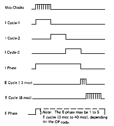
Machine cycles
Each machine cycle is made of an instruction phase and an execution phase.
The instruction phase lasts three clock cycles, the execution phase depends on the
instruction to be executed and can be one to three clock cycles long.
Each clock cycle consists of eight clock pulses.
- Instruction phase
- 1. cycle
The contents of register 0 (the instruction pointer) is loaded into the SAR.
- 2. cycle
The instruction addressed is transferred from RWS or ROS into the instruction
register.
- 3. cycle
The SAR is incremented by two and written back into register 0.
- Execution phase
The instruction fetches will be executed; only RWS can be addressed during this
phase.
The processor can be interrupted from normal execution by I/O devices. There
are four interrupt levels:
- Level 0 - Normal execution
- Level 1 - Interrupt from the BSCA or Asynchronous Communications
Adapter
- Level 2 - Interrupt from the tape drive, disk drive, printer or Serial I/O
- Level 3 - Interrupt from the keyboard
Each interrupt level has its own set of 16 2-byte registers with register 0 as
instruction pointer. The other registers are available for general use.
Program execution starts at level 0. If more than interrupt occur the level with the
highest priority is selected first (equal to the interrupt level number).
Machine check
As soon as the processor detects an error condition execution will stop (unless
a jumper on the backplane is removed) and the PROCESS CHECK light will come
on.
There are the following possibilities for an error condition:
- Parity error
A parity error in the RDR can be triggered e.g. by non-existent memory.
A Bus In or Bus Out error during transfers can also lead to a parity
error.
- Address check
This happens either in the computer or in a peripheral device as e.g. the printer
when an odd number of device address lines are active. Only exacly one X line and
only exaclty one Y line must be active.
I/O flow control
control, put and get strobe pulses as well as op code E
indicate different parts of I/O instructions being executed.
-
A control strobe indicates a valid control data byte on the bus out lines
ready for reading by the I/O device.
-
put strobe indicates a valid data byte on the bus out lines.
-
get strobe is then generated by the I/O device as acknowledge.
-
op code E is directly decoded from the machine opcode E (the STAT
instruction) and is used for transfer of some non-data bytes from an I/O device
to the processor.

